
Welcome to the European network of Chips Competence Centres
Connecting SMEs, start-ups and innovators with semiconductor expertise, training and access to venture capital across Europe.
What do you need?
Technical expertise
Prototyping, testing, characterisation and the know-how of the competence centres.
Access expertiseAccess to capital
Connections to investors and funding opportunities across the ecosystem.
Connect with VCs
Latest News
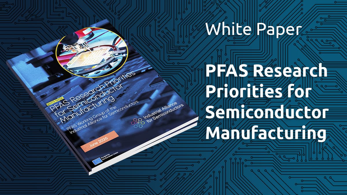
White Paper - PFAS Research Priorities for Semiconductor Manufacturing
The Industrial Alliance for Semiconductors brings together Europes key microelectronics stakeholders through dedicated working groups addressing strategic challenges. One of these groups focuses on PFAS in semiconductor manufacturing, tackling the balance between environmental concerns and industrial needs. A new white paper outlines research priorities to support this transition....

Chips Act 2.0: a shift towards demand for European chips
The European Chips Act 2.0, presented on 3 June 2026, shifts the focus to demand for European chips. ChipNL CC reflects on what this means for the Dutch semiconductor ecosystem....
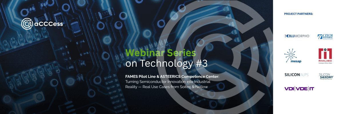
aCCCess Webinar Series - Technology Offers #3: FAMES Pilot Line & ASTEERICS Competence Center
Watch the replay of the session featuring the FAMES Pilot Line, the EuroCDP and the French Chips Competence centre ASREERICS, with real use cases from Soitec & Nellow...
Open Calls

CHIPS JU Calls: July 2026
Opens:Jul 07, 2026 09:00 CET
Closes:Sep 30, 2026 17:00 CET
New Chips JU calls now open for applications, worth over 300 million in EU funding.
The calls span the two pillars of the programme: Electronic Components and Systems (ECS), which funds research and innovation projects, and the Chips for Europe Initiative, which funds capacity building and infrastructure.

Open Access to FAMES Pilot Line
Opens:Mar 09, 2026 00:00 CET
Closes:Dec 31, 2026 23:59 CET
The FAMES Pilot Line accepts Spontaneous User Requests year-round, offering organisations rapid access to its advanced semiconductor technologies outside the annual Open-Access Calls. This pathway enables time-critical projects to move forward without waiting for the next call.
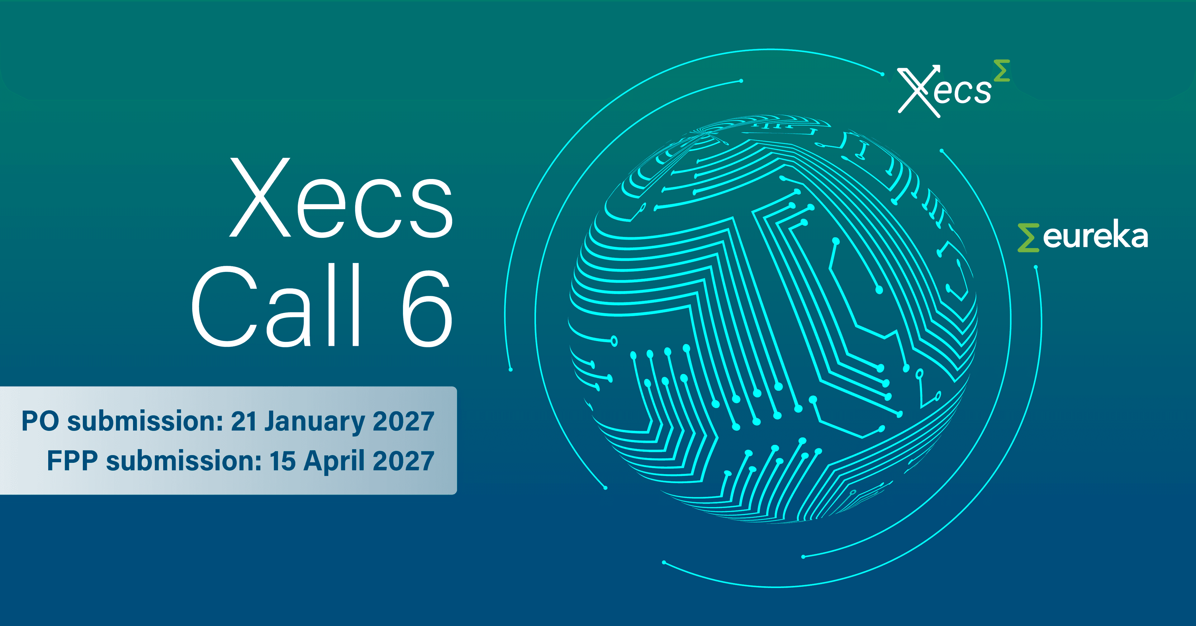
XECS Call 6
Opens:Jun 02, 2026 00:00 CET
Closes:Jan 21, 2027 17:00 CET
Xecs is an Eureka Cluster specifically designed to accelerate the pace of sustainable industrial innovation in the Electronics Components & Systems (ECS) community. Xecs intends to create an ambitious international collaboration programme. The resulting RD&I projects will generate high societal and economic impact for all those who participate in an Xecs project.
Events
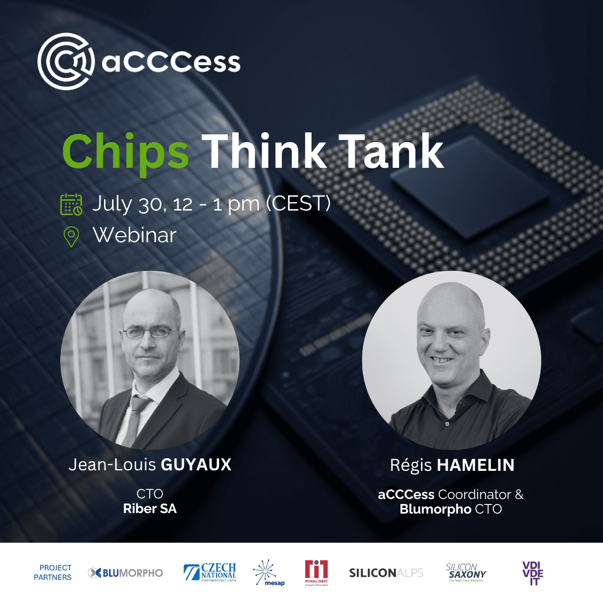
Chips Think Tank Webinar#7: Building the Materials Platform for the Future of Integrated Photonics
Jul 30, 2026 12:00 CETJul 30, 2026 13:00 CET
Webinar
Integrated photonics is entering a new phase of development, driven by the demand for higher bandwidth, lower power consumption, and the emergence of new applications in AI infrastructure, quantum technologies, telecommunications and sensing. While silicon photonics has established itself as a key platform, the next generation of photonic devices will...
Event hosted by![]()
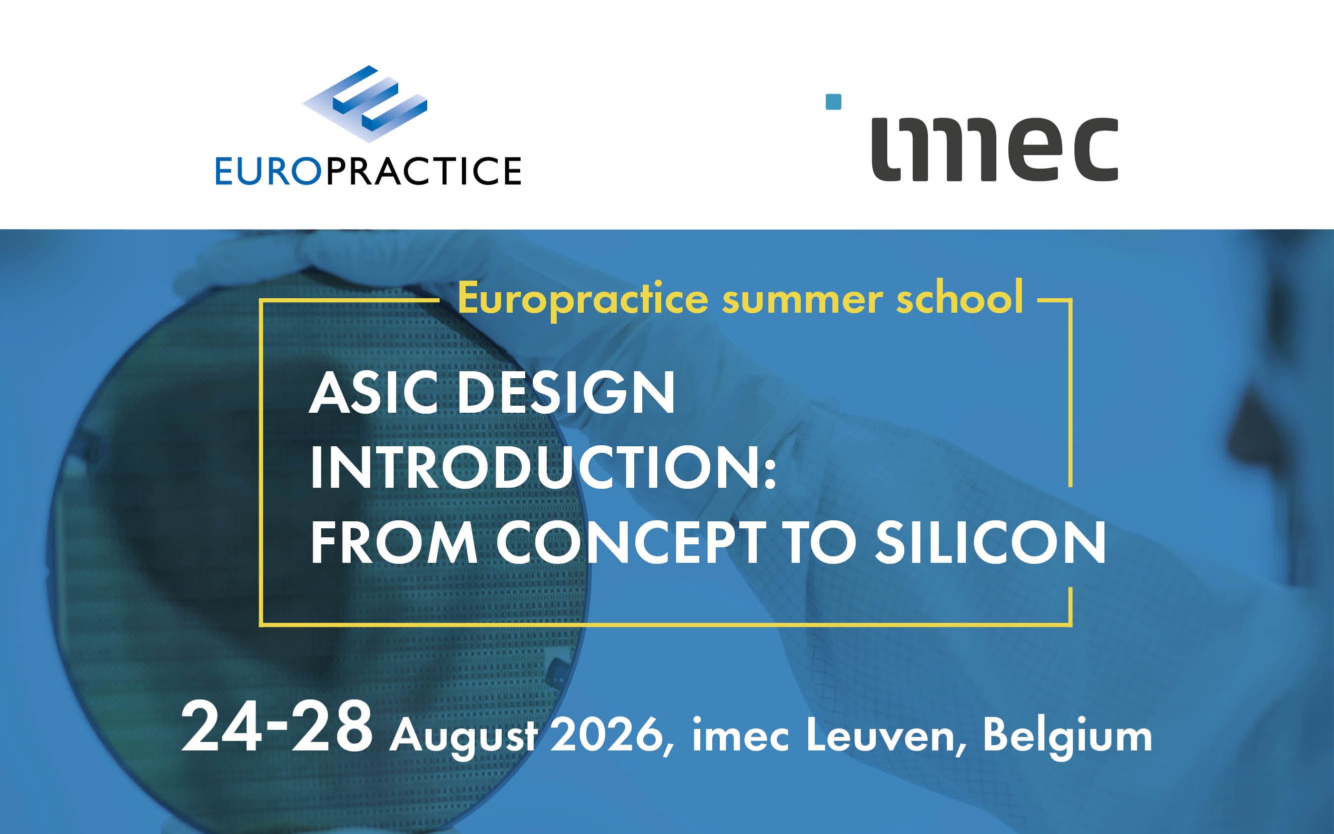
ASIC Design Introduction: From Concept to Silicon
Aug 24, 2026 09:00 CESTAug 28, 2026 12:00 CEST
Imec, Leuven, Belgium
This course will provide a thorough introduction to the ASIC design and development flow, covering multiple aspects, such as basics of Digital and Analog Design, Packaging, Test, Chiplet Integration, and IP-related challenges. All sessions will be given by experts from imec. This course is aimed at students with a professional Bachelor's...
Event hosted by

ESSERC
Sep 07, 2026 10:00 CETSep 07, 2026 12:00 CET
Palma de MallorcaSpain
The premier European forum for sharing innovations in solid-state devices and circuitsESSERC provides an annual European forum for the presentation and discussion of recent advances in solid-state devices and circuits. With the level of integration for system-on-chip design rapidly increasing, a deeper interaction among technologists, device experts, IC designers and...
Event hosted by
Latest Trends
QPerfect And University Of Strasbourg Partner To Support France's First Public Neutral-Atom Quantum Computing Platform
BTQ Technologies announced that its wholly owned subsidiary, QPerfect, has entered into a research collaboration with the University of Strasbourg in support of aQCess, France's first publicly accessible neutral atom quantum computing platform. The aQCess platform, led by co-coordinators Shannon Whitlock and Guido Pupillo at the Centre Européen de Sciences Quantiques, is targeting more than 400 qubits and is supported by the French National Strategy for Quantum Technologies.
New Quantum Material and Chip Architecture Tackle a Key Barrier to Scaling Quantum Computers Towards 1M Qubits - Semiconductor Digest
A new concept from Warwick researchers could help solve one of the biggest challenges to building large-scale quantum computers: enabling communication between quantum bits (qubits) over long distances across a single chip.
Siemens and NVIDIA Target More Verifiable AI-Driven Outcomes in Chip and PCB Engineering
(IN BRIEF) Siemens has expanded its strategic partnership with NVIDIA to advance self-verifying agentic AI workflows for semiconductor and PCB design. The collaboration combines ...

aCCCess has received funding from the European Union’s Digital Europe Chips JU under Grant Agreement No 101217840.
Funded by the European Union. Views and opinions expressed are however those of the author(s) only and do not necessarily reflect those of the European Union or [name of the granting authority]. Neither the European Union nor the granting authority can be held responsible for them.