Latest News

The European Semiconductor industry comes together: The HCHiP Collaboration Days in Budapest were a success!
The purpose of the international conference was to enhance creating a competitive semiconductor ecosystem in Hungary. The mission of HCHiP event focuses on transforming knowledge into real industrial value. Moreover, we declared the HCHiP is not a single research project, but a long-term strategic ecosystem program. That is precisely why we are building connect between research institutions, universities, industry partners, and European semiconductor networks.
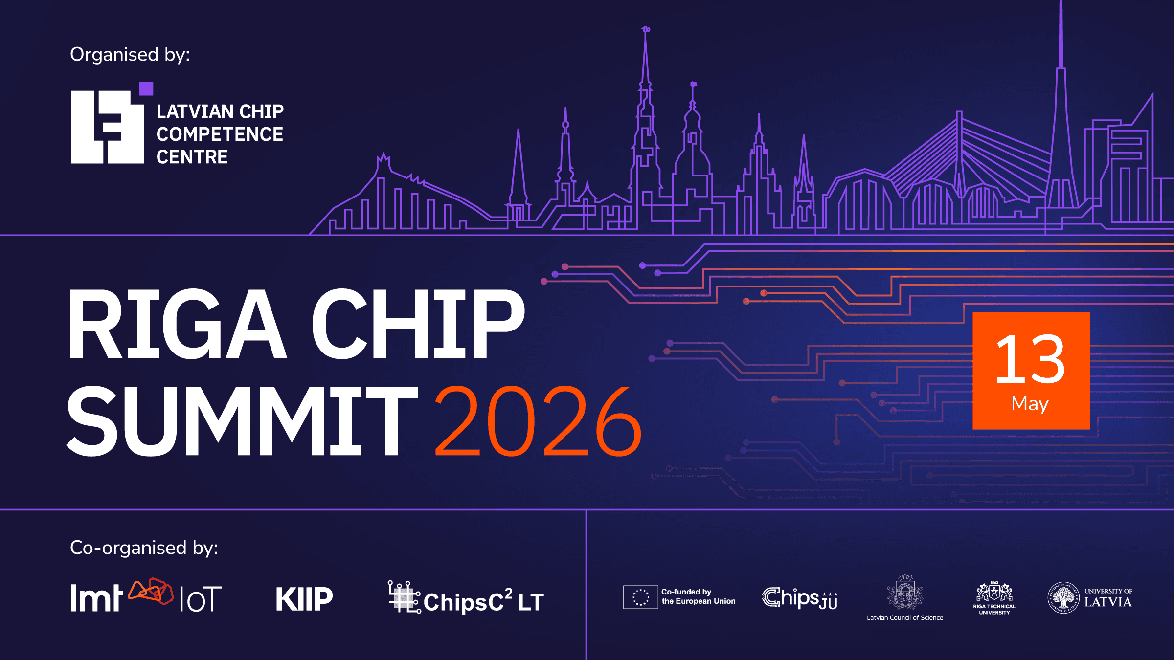
Riga Chip Summit 2026: Strengthening Europes Semiconductor Ecosystem
On 13 May 2026, the Latvian Chip Competence Centre hosted the Riga Chip Summit 2026, the first-ever semiconductor-focused summit in Latvia. The event marked a significant milestone for the Baltic and European semiconductor landscape, bringing together over 200 participants from 23 countries, including industry leaders, researchers, startups, investors, policymakers, and academic representatives from across the Baltics, Nordics, and wider Europe.
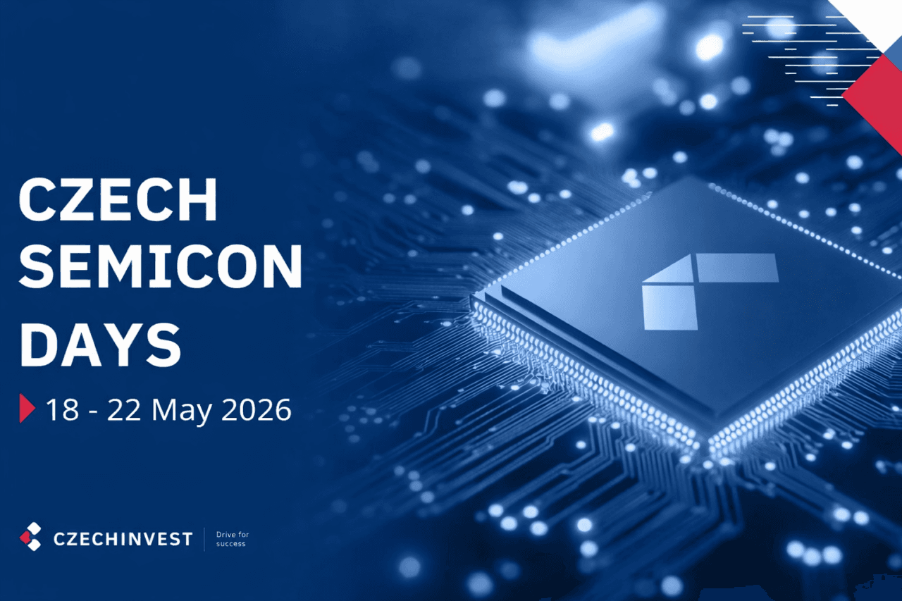
Czech Semicon Days 2026
The Czech Semiconductor Centre took part in this years Czech Semicon Days 2026 as an expert partner of the international forum organised by CzechInvest. The event, held from 18 to 20 May in Prague, Brno and Usti nad Labem, connected Czech semiconductor expertise with leading European and global partners, investors, companies, universities and public-sector representatives.
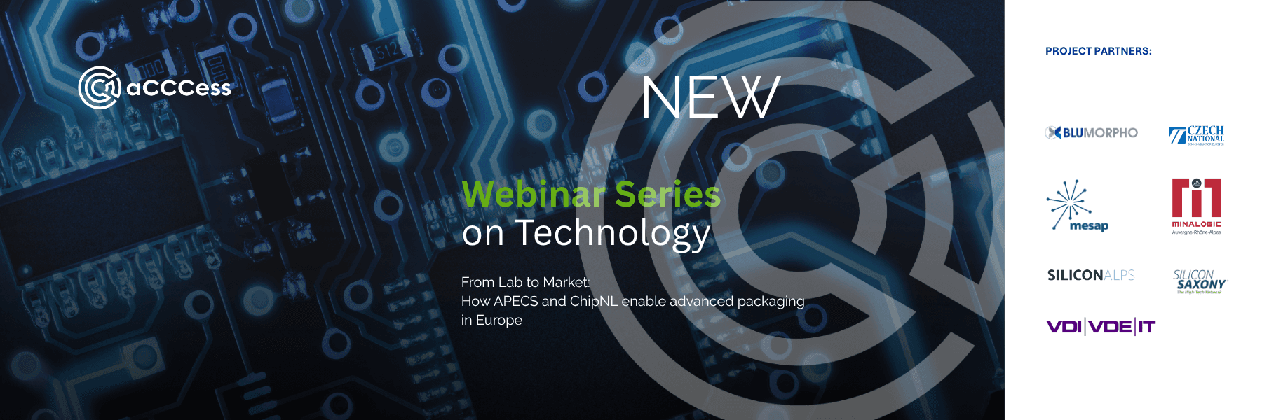
aCCCess Webinar Series Technology Offers #1
The first webinar of the aCCCess Webinar Series on Technology Offers featured the APECS Pilot Line, showcasing its advanced packaging and heterogeneous integration capabilities under the EU Chips Act. The session highlighted collaboration with the ChipNL Competence Centre and explored how joint efforts support innovation, industry uptake, and the strengthening of Europes semiconductor ecosystem.
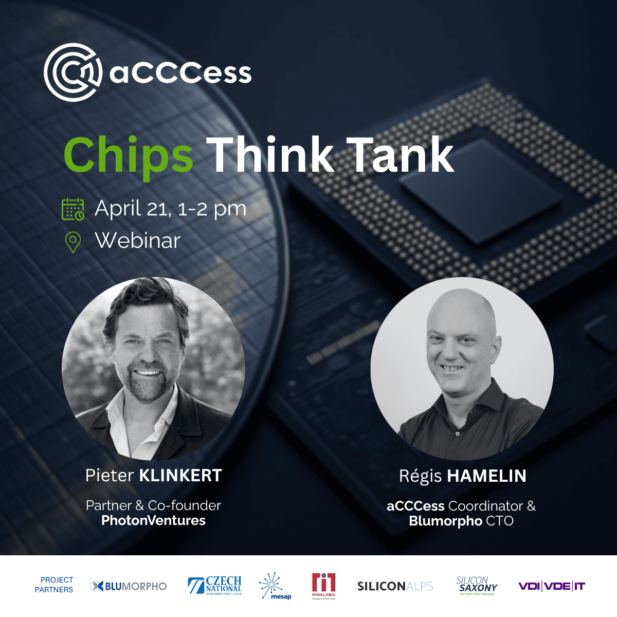
Chips Think Tank Webinar-6
Exploring the Future of Investment in Deeptech & Photonics

Chips from the North: Connecting Design and Manufacturing in Europe
On 23-24 March, the Chips from the North event in Helsinki, organised by FiCCC, brought together Europe's semiconductor community to explore available support for companies across the value chain.

ENCCC Annual Meeting: Strengthening Europes Semiconductor Network
First Annual Meeting of CCCs was held on 5-6 February in Brussels

PIXSpain Competence Centre Webpage Content Available
We are pleased to announce that the PIXSpain Competence Centre webpage is now fully available, providing a comprehensive overview of our role, activities, and ecosystem engagement within the photonics ecosystem.

Training videos on YouTube
Upskill yourself for free with the learning videos produced by the Austrian Chips Competence Center. The first are already available on YouTube and will later be part of a full online course.
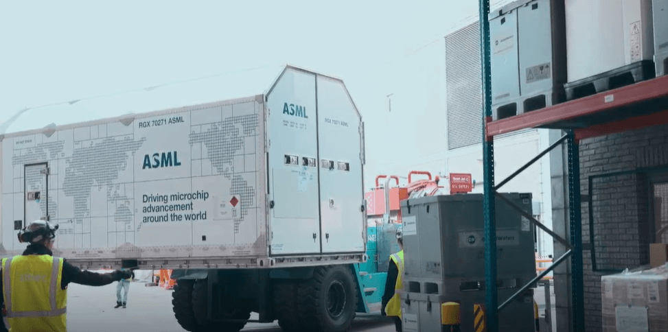
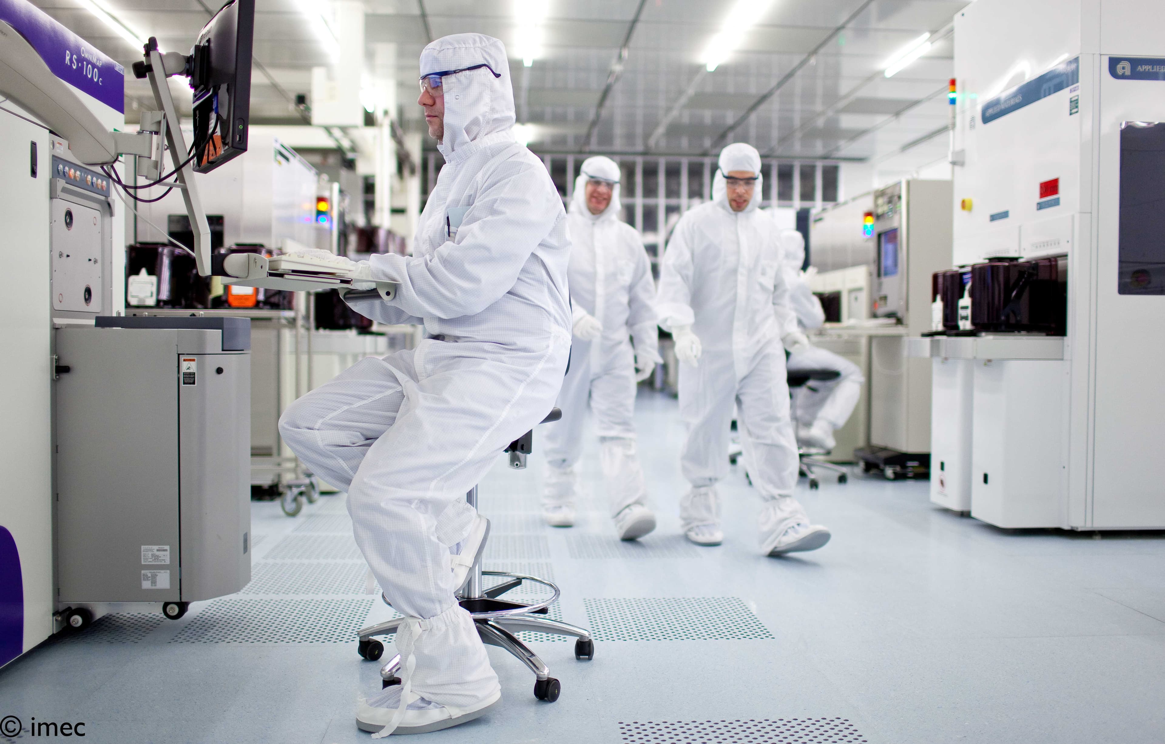
NanoIC pilot line welcomes ASML’s TWINSCAN NXT:2150i
Early November, we successfully moved ASML's TWINSCAN NXT:2150i – the most advanced deep ultraviolet (DUV) immersion lithography system available today – into imec's cleanroom. With enhanced overlay accuracy, improved critical dimension uniformity, and optimized system dynamics, the NXT:2150i supports NanoIC’s mission to push the boundaries of semiconductor scaling. What's more, with ASML’s full product portfolio being integrated into imec’s pilot line – including High-NA EUV – NanoIC can tap into the world's most advanced infrastructure for semiconductor R&D. While High-NA EUV will be used for the most demanding layers, the NXT:2150i will handle many less critical layers. Offering high throughput, the tool will accelerate imec’s capacity to develop and validate new process modules at industry-relevant dimensions, shortening learning cycles and speeding up the path from idea to prototype. Watch the video for a behind-the-scenes look at this exciting step forward ...

Chips Venture Forum 2025 Award... and the winner is Vertical Compute
The Chips Venture Forum 2025, organised by aCCCess and operated by Blumorpho in collaboration with the European Innovation Council and the European Commission, concluded on the 18 November 2025 at Messe Munich alongside SEMICON Europa bringing together Europes most promising semiconductor innovators and leading deep-tech investors.

NanoIC featured in SEMI: bridging academia and industry with pathfinding PDKs
Featured in the media From 18 to 20 November, NanoIC joined the Chips Joint Undertaking booth at SEMICON Europa, showcasing how our pilot line accelerates semiconductor innovation in Europe. Accompanying our presence at the event, SEMI.org published an in-depth article on NanoIC’s pathfinding process design kits (P-PDKs) and how they bridge the gap between academia and industry to enable next-generation chip design. The article features insights from Professor Mehdi Tahoori (Karlsruhe Institute of Technology) and Anita Farokhnejad (DTCO Program Manager at imec), explaining why these kits are critical for Europe’s semiconductor ecosystem and how they empower researchers to innovate beyond 2 nanometer. Click to read the full SEMI.org article
Pathfinding PDKs: The missing link between academia and industry in the race beyond 2nm semiconductor innovation
Featured in the media
NanoIC’s pathfinding PDKs: accelerating design for future chips beyond 2nm technology.
Advances in AI and chip architectures are driving new demands in semiconductor design, making close collaboration between academia and industry essential.
However, as we move to advanced semiconductor technology nodes, academic research has gradually drifted away from industrial practice, limiting academic researchers in driving innovation.
NanoIC aims to bridge this gap, providing pathfinding PDKs, predictive, early-access design environments, enabling researchers to simulate and optimize future chip architectures.
By restoring the link between academic innovation and industrial practice, pathfinding PDKs accelerate disruptive ideas and help build a resilient, next-generation semiconductor ecosystem.
NanoIC: A key player in solving Europe’s semiconductor talent shortage
Featured in the media

Chips Venture Forum
Are you building the future of semiconductors, AI-powered systems, advanced materials, or edge computing? Benefit from the strengths of Competence Centres across Europe by joining a vibrant ecosystem of innovators and key stakeholders. This is your chance to accelerate your ideas and connect with experts in the semiconductor value chain.

Greek chips at the heart of innovation
Launched on 1 June 2025, the Hellenic Chips Competence Centre (HCCC) is Greece’s first semiconductor hub, established through a partnership between HETiA, the Ministry of Development, and the European Chips Joint Undertaking. With €7 million in funding, HCCC aims to strengthen Europe’s technological autonomy by supporting innovation, research, start-ups, and training in chip design and testing. As part of the EU’s “Chips for Europe” initiative, HCCC connects Greek academic and industrial sectors, focusing on specialized applications. It positions Greece as a digital technology hub in Southeastern Europe. HCCC’s initial actions will be presented at the HETiA Forum in December 2025.
Enhancing chip performance
The European semiconductor sector is experiencing significant growth, fueled by increasing investments in research and development. Companies are focusing on enhancing chip performance and energy efficiency to meet the needs of various industries.
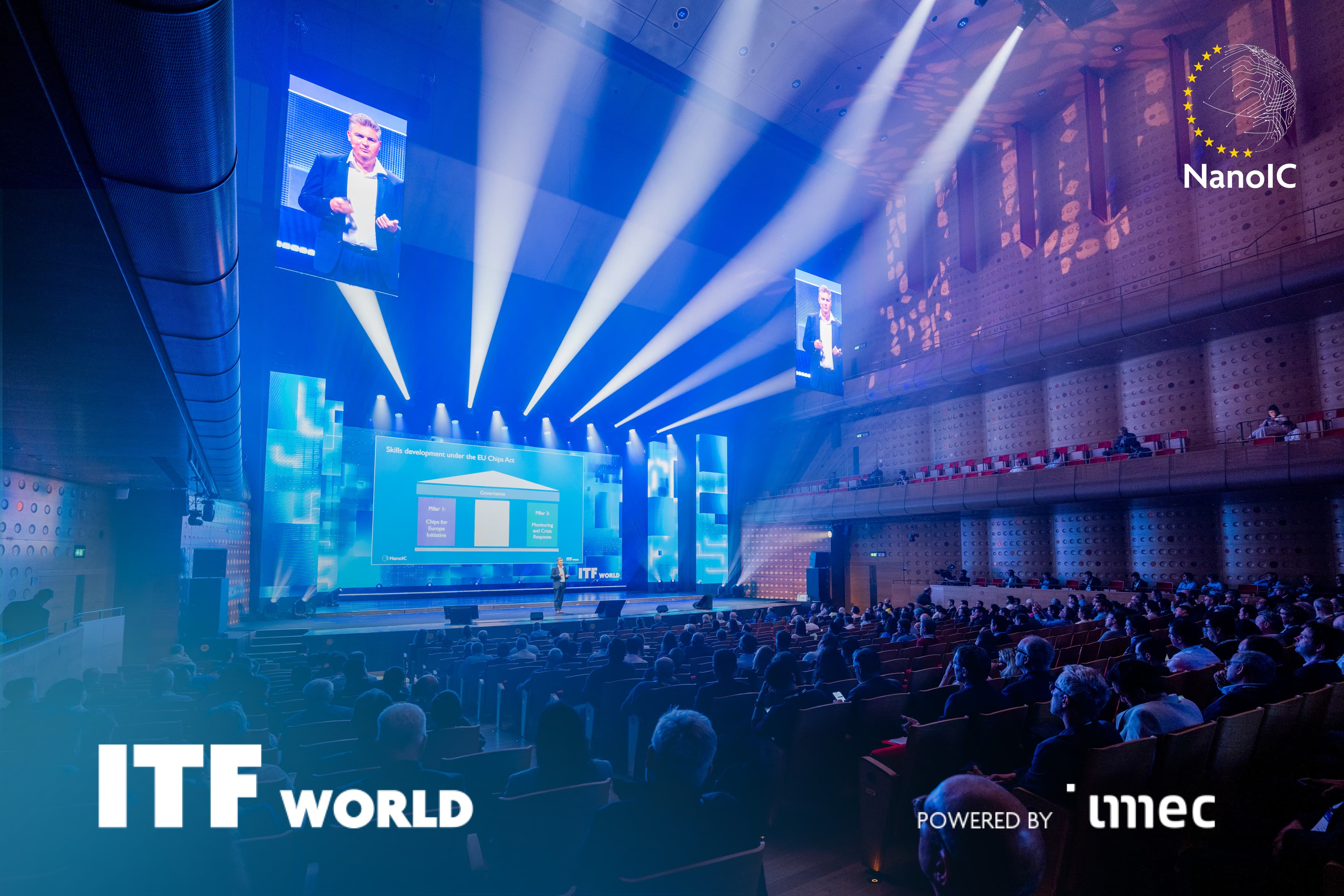
NanoIC pilot line: Europe’s strategic leap in semiconductor innovation
The German electronics magazine Markt&Technik has published a detailed feature on the NanoIC pilot line, recognizing it as a cornerstone of Europes semiconductor strategy under the EU Chips Act.
The article follows the NanoIC workshop held at ITF World 2025 in Antwerp, where the projects vision and technological roadmap were presented to a broad audience of industry leaders and policymakers.

Watch the presentations of the NanoIC pilot line workshop at ITF World 2025
Click to watch

This was the NanoIC pilot line workshop
Watch the after movie of this memorable afternoon track on the second day of ITF World 2025.

aCCCess has received funding from the European Union’s Digital Europe Chips JU under Grant Agreement No 101217840.
Funded by the European Union. Views and opinions expressed are however those of the author(s) only and do not necessarily reflect those of the European Union or [name of the granting authority]. Neither the European Union nor the granting authority can be held responsible for them.