Outer wall forksheet bridges nanosheet and CFET architectures
Research update
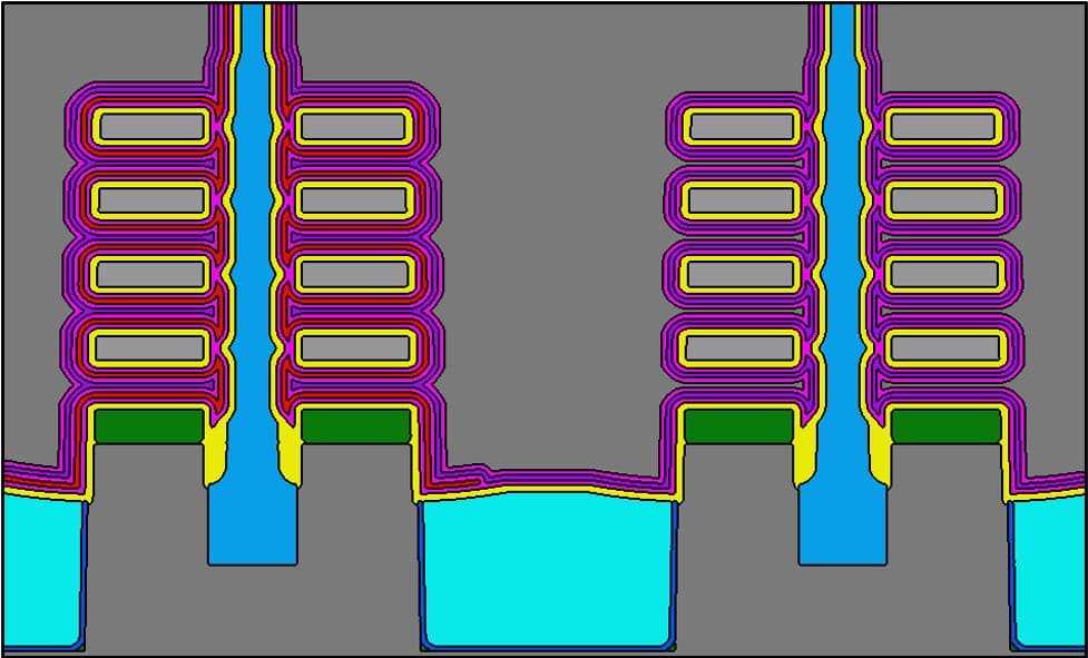
Outer wall forksheet: a scalable bridge from nanosheet to CFET for next-gen logic
As the semiconductor industry advances toward the 2nm technology node and beyond, the need for innovative device architectures becomes increasingly urgent. The outer wall forksheet, pioneered by imec and enabled by NanoIC, represents a critical step in this evolution—offering a manufacturable, high-performance successor to traditional nanosheet FETs before the complementary FET (CFET) enters the roadmap.
Unlike inner wall forksheet designs, the outer wall approach simplifies fabrication by placing the dielectric wall at the standard cell boundary and by fabricating the wall using a wall-last integration approach. This architecture not only enhances short-channel performance but also supports vertical stacking, allowing to extend the logic technology roadmap to the A10 technology node.
Discover how this breakthrough supports the NanoIC project's mission to accelerate beyond-2nm logic technologies while aligning with Europe's strategic semiconductor roadmap.
This article was originally published in EE Times.

aCCCess has received funding from the European Union’s Digital Europe Chips JU under Grant Agreement No 101217840.
Funded by the European Union. Views and opinions expressed are however those of the author(s) only and do not necessarily reflect those of the European Union or [name of the granting authority]. Neither the European Union nor the granting authority can be held responsible for them.