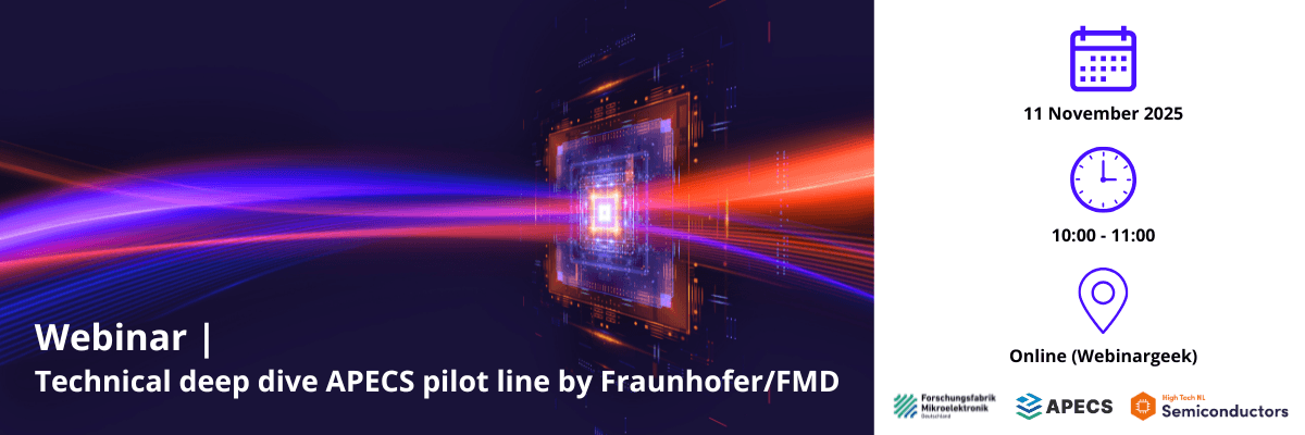
Webinar Technical deep dive APECS pilot line by Fraunhofer/FMD
EVENT DETAILS
Are you ready to dive into the cutting edge of advanced packaging and heterogeneous integration? Join us for a webinar on 11 November from 10:00-11:00 CEST that showcases the core technologies powering the APECS pilot line, your gateway to seamless process chains from design to packaging, including characterization, testing, and reliability.
In this follow-up session of the introduction webinar last September, you will discover how APECS supports next-generation applications in RF, optics, photonics, high-performance computing (HPC), and sensor systems. We'll dive into the following technology work packages:
-Quasi-monolithic integration for chiplets with different functionalities for the highest integration and ultra low-power applications
-Chiplet integration platform for 2.5 and 3D systems including functional interposers, functional integration and advanced packaging and assembly -CTR platform for the whole process chain
-STCO-design and simplifying the design of chiplet-based solutions
-Demonstrators for HPC, multi-material-sensors, photonics and RF chiplets
Whether you're a semiconductor innovator, an R&D engineer, or a technology strategist, this webinar will give you a front-row seat to how the APECS pilot line accelerates innovation in heterogeneous integration.
Don't miss your chance to get insights and connect with the APECS team of experts.

aCCCess has received funding from the European Union’s Digital Europe Chips JU under Grant Agreement No 101217840.
Funded by the European Union. Views and opinions expressed are however those of the author(s) only and do not necessarily reflect those of the European Union or [name of the granting authority]. Neither the European Union nor the granting authority can be held responsible for them.
